|
by Ek Heng NG
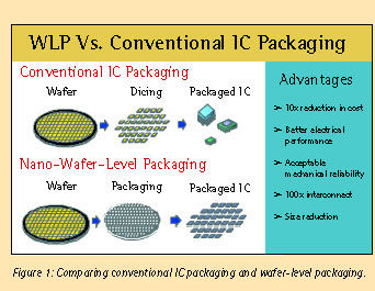
 he revolutionary concept of moving in only one step from wafer fabrication to packaged chips will turn semiconductor foundries into one-stop centres for the production of packaged integrated circuits (ICs). It is a radical departure from the current practice in which the foundry sends the wafers to other plants, sometimes to other parts of the world, for back-end packaging. With existing production technologies, wafers as big as 300mm in diameter can be continuously processed to the point where they are ready to be diced into individual packaged ICs, tested, and mounted on systems boards (Figure 1). he revolutionary concept of moving in only one step from wafer fabrication to packaged chips will turn semiconductor foundries into one-stop centres for the production of packaged integrated circuits (ICs). It is a radical departure from the current practice in which the foundry sends the wafers to other plants, sometimes to other parts of the world, for back-end packaging. With existing production technologies, wafers as big as 300mm in diameter can be continuously processed to the point where they are ready to be diced into individual packaged ICs, tested, and mounted on systems boards (Figure 1).
 Although wafer-level packaging (WLP) has begun to gain momentum in the semiconductor industry, Singapore's WLP at the nanoscale represents the first pioneering research of its kind. Known as nano-wafer-level packaging (nano-WLP), this groundbreaking research project under Temasek Professor Rao Tummala is an international collaboration among the National University of Singapore, the Institute of Microelectronics, Singapore, and the Georgia Institute of Technology, United States.
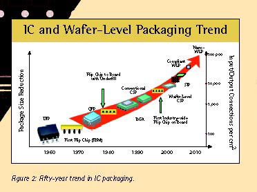
Nano-WLP pushes technology to new levels with the number of connections and the bandwidth it provides to the end-product system. It has come a long way from the first chunky-chip packaging of the 1960s (Figure 2). Knowledge of material processes and properties at the nanoscale will inevitably bring about unprecedented advances in electrical, mechanical, environmental and thermal characteristics. These, in turn, will result in IC and systems packaging that make optimal utilisation of the chip's intrinsic computational speed.
As a direct consequence of research efforts to bring nanoscale packaging to the wafer level, future systems will incorporate a number of convergent technologies, both at IC and at systems level, so as to be much smaller and more affordable. Nanoscale research is timely in view of the semiconductor industry's race towards chips with features less than 100 nanometres in at least two dimensions at the back-end wiring level. Next comes demonstration of the viability of this new wafer-levelmanufacturing concept that can potentially reduce the number of process operations per chip by more than three orders of magnitude when compared to the current sequential wire-bonding process for attaching packaging ICs.
 Time and cost savings in manufacturing are just two examples of the many possible benefits arising from this research programme. Successful proof of concept will lead to a new generation of eversmaller products with unlimited connections between the devices and the rest of the system, offering higher performance and newfound applications. Time and cost savings in manufacturing are just two examples of the many possible benefits arising from this research programme. Successful proof of concept will lead to a new generation of eversmaller products with unlimited connections between the devices and the rest of the system, offering higher performance and newfound applications.
From a manufacturing perspective, the research will lead to the development of the smallest IC package to date, ushering in a new generation of truly chip-size packages, both using nanoscale interconnection and packaging technologies. Because both are done at the wafer level in the wafer foundry in one set of parallel steps, costs for packaging, electrical testing, and burn-in-reliability testing will be significantly reduced. The short nano-interconnection will also greatly enhance electrical performance. In addition, the potential exists for greater savings by eliminating the need for underfilling around solder joints, a widespread practice today.
The multidisciplinary team of up to 50 researchers and postgraduate students from the three collaborating institutions is faced with tremendous challenges. The viability of the nano-WLP will be proven in two phases - first at 100µm pitch, followed by 20µm pitch. In terms of interconnections, the research goal is to increase the current industry figure of 340 I/Os (input/output) to 1,000 in the first phase and in excess of 10,000 I/Os in the second phase. A follow-up programme is expected to bring these connections to true nanoscale via nanotubes, nanowires and single-crystal nanowire connections. The challenge can be seen in terms of the size of the interconnections, which can be reduced from the current 300µm to 30µm in the first phase, 6-8µm in the second phase, and 50-100nm in the follow-up research.
Besides seeking to break new ground in electrical design and gaining an understanding of nanostructured materials and nanointerconnection processes, the other areas of research the team has identified are: high-density board; thermo-mechanical design, modelling and analysis; test and burn-in at the wafer level; and developing an integrated test bed for 100µm-pitch prototype WLP systems.
In developing electrical designs, to minimise use of cycle-time-consuming error correction algorithms, issues such as cross-talk, skin effect, reflections, switching noise, electromigration and eye patterns need to be overcome. Using modelling and experimental techniques, the team members will study various options in electrical design to support digital and radio frequency signals at 20-50GHz, as well as to supply up to 200 watts of power to chips without signal interference.
As ICs continue to offer more features and better performance at yet lower cost and smaller size, the need for an innovative and reliable interconnect technology becomes more critical. Industry studies show that most existing interconnect technologies today, even with dramatic improvement, cannot address the reliability of ultra-fine-pitch interconnections.
Hence, a compelling need presents itself to understand the thermo-mechanical design requirements, failure mechanisms and reliability of such interconnects. The team is investigating the benefits of compliant and rigid interconnections. It is also identifying promising materials systems for use in 20µm-pitch interconnects, and producing the materials in sufficient quantities for evaluation. Materials will be characterised for tensile strength, hardness, fracture toughness, fatigue and electrical properties.
One of the goals of this Temasek Professorship project is to develop fine-pitch, low-cost interconnect technologies for ultrahigh-density WLP. Current WLPs run at a pitch of 30-400µm whereas researchers for this project are exploring technologies for 2-100µm pitch initially, which must be designed to meet electrical, thermal and mechanical requirements. Wiring connections between chip and package can be made shorter to minimise or eliminate the deleterious effects associated with other WLP technologies.
After production, the WLP must be evaluated. Individual IC-level test and burn-in are expensive processes. One objective of the project is thus to develop less costly new paradigms that will provide faster turnaround. The team has to contend with such issues as the selection of appropriate materials, the integration of different components in the test system (for example, test processors and test fixtures), as well as fabrication methods for that test system.
Finally, an integrated wafer-level test-bed prototype to demonstrate the reliability of the 100µm-pitch wafer-level-packaged system will have to be built. Provision must also be made to develop a 100µm board in which to assemble the nano-WLP to assess its functionalities fully.
For more information contact Rao Tummala at rtummala@ee.gatech.edu
|