|
by Yihong WU
 ry peeling off the carbon in natural graphite layer by layer and making each one stand up in alignment on a base. Scientists at the National University of Singapore and the Data Storage Institute have realised such a result using a novel chemical vapour-deposition method. They have dubbed the carbon structure thus obtained a carbon nanowall, which joins the well-known fullerene (carbon arranged in spheres or tubes) and nanotube (microscopic carbon tubes) to form a family of carbon nanostructures. ry peeling off the carbon in natural graphite layer by layer and making each one stand up in alignment on a base. Scientists at the National University of Singapore and the Data Storage Institute have realised such a result using a novel chemical vapour-deposition method. They have dubbed the carbon structure thus obtained a carbon nanowall, which joins the well-known fullerene (carbon arranged in spheres or tubes) and nanotube (microscopic carbon tubes) to form a family of carbon nanostructures.
Current research has made it possible for the first time to grow carbon nanostructures with zero dimensionality (0D) to two dimensions (2D) in a well-controlled fashion.
The alchemist - who in ancient times dreamt of finding a way to turn lead into gold - would today probably prefer to turn graphite into diamonds. Diamonds and pencil "lead," like all matter, are made up of atoms. To turn graphite into a diamond seems possible because both are made up of carbon atoms. However, this requires changing the arrangement of carbon atoms.
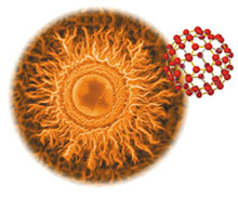
The diamond, one of the hardest known materials, comprises carbon atoms in a tetrahedral structure, in which each atom bonds to four other atoms with all angles being equal to 109.47o. We use graphite every day as the main component of the core of pencils. Carbon atoms make up graphite too, but in a two-dimensional layered structure. Each layer is a hexagonal graphene sheet on which three nearest neighbouring atoms surround each carbon atom with all three angles equal to 120o. A weak force between the adjacent layers makes graphite easily scrubbed off layer by layer, and so we use a pencil to write on paper. Diamond and graphite constitute the two most important types of carbon in the natural form, or so-called bulk carbon.
Once atoms form chemical bonds, their properties cannot be easily altered in a normal environment. Two choices are present if one wants to have a carbon material that would behave differently from either diamond or graphite. One is to form artificial carbon molecules or structures different from the diamond or graphite structure.
Depending on the kind of properties looked for, one can alter naturally formed bulky materials by controlling the movement of the electrons inside the material. However, electrons inside a conducting material are like the water inside the ocean - great difficulties lie ahead for the person who wishes to control the motion of water at the ocean's centre. It would be much easier to control the motion of water inside a significantly smaller container.
Relative size matters - and the same situation also applies to electrons inside a conducting material. The second approach then is to "cut" bulk materials into extremely small units so that the electrons inside the small unit will "experience" a different environment from those in the bulk counterpart. Because these units are measured in the nanometre (a billionth of a metre) range, they are called nanostructures. How fine one can cut a material into small pieces depends very much on how good one's skills and tools are, but in general it becomes difficult when the dimension shrinks to below sub-100nm. This approach is referred to as the top-down approach.
Carbon constitutes a field in which nanotechnology has had much success, thanks to the bottom-up approach. This approach allows researchers to control the motion of electrons easily without starting from raw diamond or graphite materials. Carbon can be "grown" into different forms either in terms of its chemical bonding or its dimensionality. Both fullerenes and carbon nanotubes represent unusual form of carbons in the nanometre range.
The researchers have recently succeeded in growing well-aligned 2D carbons (dubbed carbon nanowalls) on various substrates using microwave-plasma-enhanced chemical vapour deposition. They found that the presence of a 2D electric field is the key to growing carbon nanowalls instead of nanotubes. A series of experiments have been carried out to verify this observation. As one of the examples, when a liquid droplet of metal is put inside a plasma environment, a unique electrical field distribution would form. This field, in turn, will determine the orientation of the carbon nanowalls.
As a different form of carbon nanostructure, in particular its two-dimensionality, the nanowall may provide an excellent opportunity for scientists to explore a new physics of carbon nanostructures with open boundaries. From the practical point of view, the scientists find carbon nanowalls extremely interesting because of their large surface areas. Focusing on this last aspect, they have grown a dozen nanostructured materials on carbon nanowall templates.
Nanowalls may have potential practical application in batteries, gas sensors, catalysts, light emission/detection, field emission and biomedical devices. In fact, the group has found that the threshold field emission field of carbon nanowalls is much lower than that of carbon nanotubes, which makes them very promising for field emission displays and other miniaturised electron sources.
The NUS researchers have successfully grown well-aligned carbon nanowalls with a thickness of a few nanometres and a lateral size in the micrometre range on various types of substrates. The nanowalls exhibit a remarkably different surface morphology as compared to fullerenes and carbon nanotubes, in particular their two-dimensionality and their high surface area. So far the team has focused on the latter aspect and developed a templating method to fabricate a class of nanostructured materials based on the novel surface morphology of the carbon nanowalls. Exploration of application in other fields is under way. The researchers have also succeeded very recently in growing other types of materials with similar structure of the carbon nanowalls.
For more information contact principal investigator Yihong Wu at elewuyh@nus.edu.sg
|